
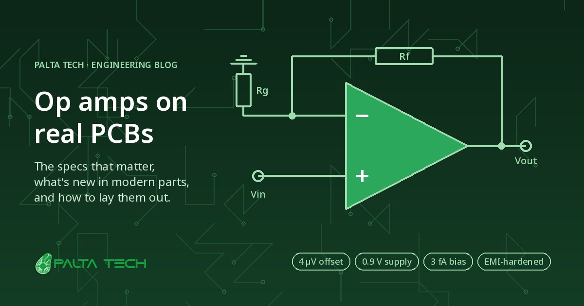
The operational amplifier is probably the most reused building block in analog electronics. On our boards it measures motor current, conditions sensors, drives ADCs and filters noise. Picking one is still a balancing act between a dozen specs, and over the last decade the parts themselves have changed a lot. This article walks through the specs that matter, the new features in modern op amps, and the PCB layout habits that decide whether a good part performs well on your board.
By the end of this article, you'll understand:
- Which op amp specs actually limit your circuit, and why
- Where op amps show up in power electronics and IoT hardware
- What modern parts offer: zero-drift, EMI hardening, sub-1 V supplies and more
- The layout rules we follow to keep precision and stability on a real PCB
The Specs That Matter
A good starting point is the classic talk "The various specs of op-amps", first presented at an EE Times analog conference in 1997. Its main idea still holds: there is no best op amp. There are many separate "spec ladders," and every real part sits high on some and low on others. Your job is to find out which ladders your circuit actually climbs.
The Perfect Op Amp vs. Real Parts
The perfect op amp is free, has infinite gain and bandwidth, no noise, no offset and no input current. Real parts fall short on each of those in their own way. These are the specs we check first:
| Spec | What it means | Why it bites on a board |
|---|---|---|
| Offset voltage and drift | The input voltage error when the output should be zero, and how it changes with temperature and time. | Multiplied by the noise gain, it lands on top of every small DC signal you measure. |
| Input bias current | The small current each input pin draws or sources. | Flowing through high source resistance, it becomes an extra offset voltage. |
| Gain-bandwidth product | The frequency at which open-loop gain falls to 1. | At closed-loop gain G, usable bandwidth is roughly GBW / G, and accuracy degrades well before that. |
| Slew rate and settling time | Large-signal speed, and the time to settle within an error band after a step. | A multiplexed ADC input can step from rail to rail. If the amp hasn't settled, the sample is wrong. |
| Noise | Input-referred voltage and current noise, in nV/√Hz and pA/√Hz. | It is multiplied by the closed-loop gain. At high gain it can cost several bits of a 16-bit ADC. |
| CMRR and PSRR | How well the amp rejects common-mode signals and supply ripple. | Both fall with frequency. Switching-regulator ripple at hundreds of kHz gets much less rejection than DC. |
| Input and output range | How close to the rails the inputs and output can operate. | On a 3.3 V supply, losing 1.5 V to headroom leaves very little signal range. |
| Stability and minimum gain | Some parts are only stable above a minimum closed-loop gain or with limited capacitive load. | A buffer that oscillates at 20 MHz looks like a noisy, warm, slightly wrong DC output on a multimeter. |
Then and Now
The 1997 talk listed the range real parts covered at the time. Here is how far the best modern parts have moved some of those limits. Each figure comes from the datasheet of a part in production today:
| Spec | Range in 1997 | Modern example |
|---|---|---|
| Offset voltage | 0.5 mV to 10 mV | ±4 µV max, 0.01 µV/°C max drift (ADI ADA4523-1) |
| CMRR / PSRR | Up to about 130 / 145 dB | 160 dB / 168 dB typical (ADI ADA4523-1) |
| Input bias current | Down to 10 fA, in slow parts | About 3 fA typical with 500 MHz GBW (ADI LTC6268) |
| Supply current | From about 1 mA | 500 nA typical per channel (TI TLV8541) |
| Minimum supply | "Low voltage" meant CMOS at a few volts | 0.9 V, with zero-drift precision (ADI MAX40108) |
Keep in mind: no single part has all of these numbers. The femtoamp part draws 16 mA, and the nanopower part has an 8 kHz bandwidth. The spec ladders are still there. They are just taller.
Where Op Amps Live on Our Boards
In the power electronics and IoT products we design, op amps usually do one of these jobs:
- Current sensing across a shunt resistor in motor drives, chargers and DC-DC converters.
- Sensor front ends for thermistors, strain-gauge bridges, photodiodes and 4–20 mA loops.
- ADC drivers that charge the sampling capacitor of a SAR ADC quickly and settle before the conversion.
- Anti-aliasing and active filters such as Sallen-Key stages in front of the ADC.
- Reference and mid-supply buffers that create a stiff virtual ground on single-supply boards.
When the common-mode voltage is high, for example a shunt on the high side of a 48 V bus, a plain op amp in a difference-amplifier circuit is limited by how well its resistors match. That is where a dedicated current-sense amplifier or instrumentation amplifier earns its place.
Worked Example: Low-Side Current Sensing
Say a motor drive measures phase current with a 2 mΩ shunt, and we care about accuracy down to 0.5 A. At that current the shunt drops only 1 mV.
- A general-purpose amp with a 1 mV offset adds an error as large as the signal itself: 100%.
- A zero-drift amp with a 4 µV maximum offset adds 0.4%, and that number barely moves with temperature.
You could raise the shunt value instead, but at 30 A a 20 mΩ shunt dissipates 18 W. With a modern zero-drift amp you keep the small shunt, the low losses and the accuracy.
What's New in Modern Op Amps
Beyond better numbers, newer op amps add features that used to take extra parts on the board, or that didn't exist at all.
Zero-Drift Goes Mainstream
In 1997, the answer to "low offset, low drift" was a chopper amplifier, with the warning "slow and costly." Today's zero-drift parts use auto-zeroing or chopping internally and are neither. The ADA4523-1 runs from 4.5 V to 36 V with ±4 µV maximum offset, 0.01 µV/°C maximum drift, 4.2 nV/√Hz noise and 5 MHz GBW. That is precision and reasonable speed in one part.
Zero-drift amps still have side effects you should check in the datasheet:
- Ripple and spurs at the internal chopping frequency, which can alias into a sampled signal.
- Input bias current with small spikes from switch charge injection, higher than a plain CMOS input.
- Slower recovery from overload than a classic bipolar amp in some parts.
EMI-Hardened Inputs
An op amp's input transistors rectify RF. A nearby BLE or LTE radio, or the fast edges of a GaN or SiC half-bridge, shows up as a DC offset shift that no amount of low-frequency filtering will remove. Many modern parts integrate RF filters on their inputs and specify an EMIRR (EMI rejection ratio). For example, the ADA4177 specifies about 70 dB of rejection at 1000 MHz and 90 dB at 2400 MHz. TI's OPA2991 filters both its inputs and its supply pins.
Rail-to-Rail Without the Crossover
Classic rail-to-rail input stages use two input pairs, one for each rail, and hand over between them somewhere in the middle of the range. In that handover region the offset jumps and distortion rises. Parts like TI's OPA320 use an internal charge pump to power a single input pair above the positive rail. The result is a common-mode range that extends 100 mV beyond both rails with no crossover region, and a CMRR of 114 dB (typical) across the whole range. This matters for ADC drivers that swing across the full scale.
MUX-Friendly Inputs
Many precision amps have clamp diodes between their inputs. When a multiplexer switches channels, or when the amp is used as a comparator, a large differential voltage turns those diodes on. Input current then spikes and settling suffers. "MUX-friendly" parts such as the OPA2991 accept a differential input up to the supply rails. TI states it can also be used open loop as a comparator. The OPA2991 also runs from 2.7 V to 40 V with rail-to-rail inputs and outputs, which makes it a good fit for 12 V and 24 V industrial boards.
Built-In Overvoltage Protection
Inputs that connect to the outside world, such as sensor connectors and long cables, eventually see voltages beyond the supply. The traditional fix is a series resistor and clamp diodes. Both add noise, and their leakage adds offset. The ADA4177 integrates protection that tolerates input voltages 32 V beyond either supply rail by limiting the input current internally. In many designs that removes the external clamp network.
Sub-1 V Supplies and Nanopower
Battery-powered IoT nodes changed what "low power" means. The MAX40108 runs from 0.9 V to 3.6 V on 25.5 µA (typical), with 1 µV typical zero-drift offset and a shutdown mode. Its WLP package measures 1.22 mm × 0.92 mm. For slow signals, TI's TLV8541 draws about 500 nA per channel with 8 kHz of bandwidth. Over a multi-year battery life, an always-on sensor front end at that current is negligible.
The low-cost end improved too. Parts like TI's TLV9001 give you rail-to-rail input and output, 1 MHz GBW and about 60 µA per channel from 1.8 V to 5.5 V, for tens of cents in volume. On a 3.3 V board, there is little reason to choose the older part.
Femtoamp Inputs at High Speed
The 1997 guide warned that low bias current came with noise, speed and temperature trade-offs. The LTC6268 combines a bias current of a few femtoamps (typical) with 500 MHz GBW and 4.3 nV/√Hz noise. That is the combination you want for photodiode transimpedance amplifiers and high-impedance sensors. The cost is power: it draws about 16 mA.
PCB Layout Rules
The original talk didn't cover layout, but on real boards this is where most op amp problems come from. A datasheet number only holds if the PCB doesn't undo it. These are the rules we apply.
Decoupling and Grounding
- Put a 100 nF ceramic capacitor at each supply pin, with vias straight into a solid ground plane. Add a larger bulk capacitor nearby.
- Use one continuous ground plane. Separate analog and power circuits by placement, not by cutting the plane, and never route a signal across a gap in its return path.
- Remember that PSRR falls with frequency. Filter supply ripple from switching regulators with an RC or ferrite-bead stage before precision amps.
Keep the Inverting Node Small
Stray capacitance on the inverting input forms a pole with the feedback resistor. That adds phase shift, which shows up as peaking, ringing or outright oscillation, especially with fast amps.
- Place the feedback and gain resistors right at the op amp pins and keep that trace short.
- For high-speed parts, remove the ground and power planes under the inverting input and feedback components.
- If you use large feedback resistors, a small capacitor across the feedback resistor restores phase margin.
Driving Capacitive Loads
Most op amps don't like driving capacitance directly. Cables, ADC inputs and large filter capacitors all reduce phase margin. Add a small isolation resistor, typically 10 Ω to 100 Ω, in series with the output, and close the feedback from the op amp side of it. For SAR ADC drivers, the datasheet of the ADC usually recommends a specific RC between the driver and the input.
High-Impedance Inputs and Guarding
At picoamp and femtoamp levels, the PCB itself becomes the leakage path. FR-4, solder mask, flux residue and humidity all leak more than a modern CMOS input.
- Surround the input trace with a guard ring driven at the same potential as the input, so there is no voltage across the leakage path.
- Clean the board thoroughly after assembly, and consider conformal coating for humid environments.
- For the most sensitive nodes, connect the input in the air or on a PTFE standoff instead of on the board.
Precision DC: Thermocouples and Kelvin Sensing
Every junction of dissimilar metals is a thermocouple: copper traces, solder, component leads and the resistor element itself. Their voltages can easily reach the microvolt level, which is the whole offset budget of a zero-drift amp.
- Route both inputs symmetrically, with the same number and type of junctions, so their thermal voltages cancel.
- Keep precision inputs away from hot parts like MOSFETs, regulators and shunts carrying high current.
- Connect to current shunts with Kelvin traces from the inner sense pads, and route them as a tight differential pair to the amplifier.
- Place the input RC filter at the amplifier, not at the shunt.
Living Next to a Power Stage
In our motor drives and converters, op amps sit centimeters away from switch nodes that slew at tens of volts per nanosecond. Capacitive coupling from those nodes into a high-impedance trace injects current spikes straight into the input.
- Keep analog inputs away from switch nodes and gate-drive loops, and never route them on a layer directly above or below one.
- Make sure high power return currents don't flow under the analog section.
- Choose EMI-hardened parts and add input RC filters with a corner well above your signal bandwidth.
- If an output feeds an ADC in the controller, sample in sync with the PWM, away from switching edges.
An Updated Selection Guide
The 1997 talk ended with a selection guide. Here is our version for today:
| Need | Answer in 1997 | What we reach for today | Watch out for |
|---|---|---|---|
| Low offset and drift | Chopper amp (slow, costly) | Zero-drift CMOS, 5 MHz-class and up to 36 V | Chopping spurs, bias current spikes |
| Low bias current | CMOS or JFET input | Femtoamp CMOS, even at hundreds of MHz | PCB leakage, power draw |
| Cheap, general purpose | LM324 | Low-cost RRIO CMOS (5.5 V) or 40 V RRIO CMOS | Offset in the millivolt range |
| Low power, low voltage | CMOS | Nanopower and sub-1 V parts with shutdown | Bandwidth in the kHz range, higher noise |
| Harsh environment | External clamps and filters | EMI-hardened, overvoltage-protected inputs | Check EMIRR at your radio's frequency |
Conclusion
The op amp is far from the perfect part in the textbook. But in the last decade, zero-drift precision became affordable, inputs learned to survive RF and overvoltage, and supplies dropped below one volt. The process is the same as in 1997: list the specs your circuit really depends on, find the part that ranks high on those, then lay out the board so it doesn't take that performance away. The old talk's last piece of advice also still holds: call the manufacturers' application engineers. They know their parts better than any datasheet.